- 您现在的位置:买卖IC网 > Sheet目录364 > SST49LF008A-33-4C-EIE-T (Microchip Technology)IC FLASH FWH 8MBIT 33MHZ 40TSOP
�� �
�
�8� Mbit� Firmware� Hub�
�A� Microchip� Technology� Company�
�SST49LF008A�
�Data� Sheet�
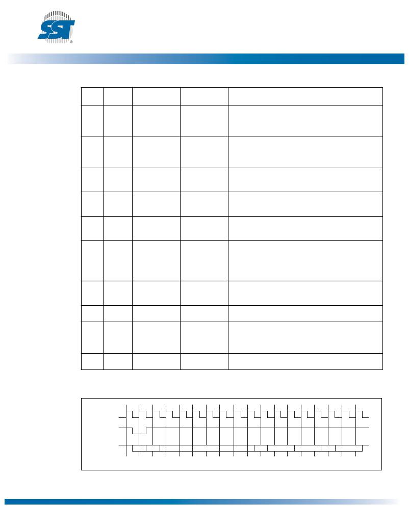
�Table� 4:� FWH� Write� Cycle�
�Clock�
�Field�
�Field� Contents�
�FWH[3:0]�
�Cycle�
�1�
�Name�
�START�
�FWH[3:0]� 1�
�1110�
�Direction�
�IN�
�Comments�
�FWH4� must� be� active� (low)� for� the� part� to� respond.� Only�
�the� last� start� field� (before� FWH4� transitions� high)� should�
�be� recognized.� The� START� field� contents� indicate� a� FWH�
�memory� Read� cycle.�
�2�
�IDSEL�
�0000� to� 1111�
�IN�
�Indicates� which� SST49LF008A� device� should� respond.�
�If� the� IDSEL� (ID� select)� field� matches� the� value�
�ID[3:0],� then� that� particular� device� will� respond� to� the�
�whole� bus� cycle.�
�3-9�
�IMADDR�
�YYYY�
�IN�
�These� seven� clock� cycles� make� up� the� 28-bit� memory�
�address.� YYYY� is� one� nibble� of� the� entire� address.�
�Addresses� are� transferred� most-significant� nibble� first.�
�10�
�IMSIZE�
�0000� (1� byte)�
�IN�
�This� size� field� indicates� how� many� bytes� will� be� trans-�
�ferred� during� multi-byte� operations.� The� FWH� only�
�supports� single-byte� writes.� IMSIZE=0000b�
�11�
�DATA�
�YYYY�
�IN�
�This� field� is� the� least-significant� nibble� of� the� data� byte.�
�This� data� is� either� the� data� to� be� programmed� into� the�
�flash� memory� or� any� valid� flash� command.�
�12�
�13�
�DATA�
�TAR0�
�YYYY�
�1111�
�IN�
�IN� then� Float�
�This� field� is� the� most-significant� nibble� of� the� data� byte.�
�In� this� clock� cycle,� the� master� (Intel� ICH)� has� driven� the�
�then� float� bus� to� all� ‘1’s� and� then� floats� the� bus� prior� to�
�the� next� clock� cycle.� This� is� the� first� part� of� the� bus� “turn-�
�around� cycle.”�
�14�
�TAR1�
�1111� (float)�
�Float� then� OUT� The� SST49LF008A� takes� control� of� the� bus� during� this�
�cycle.� During� the� next� clock� cycle� it� will� be� driving� the�
�“sync”� data.�
�15�
�RSYNC�
�0000�
�OUT�
�The� SST49LF008A� outputs� the� values� 0000,� indicating�
�that� it� has� received� data� or� a� flash� command.�
�16�
�TAR0�
�1111�
�OUT� then� Float�
�In� this� clock� cycle,� the� SST49LF008A� has� driven� the� bus�
�to� all� then� float� ‘1’s� and� then� floats� the� bus� prior� to� the�
�next� clock� cycle.� This� is� the� first� part� of� the� bus� “turn-�
�around� cycle.”�
�17�
�TAR1�
�1111� (float)�
�Float� then� IN�
�The� master� (Intel� ICH)� resumes� control� of� the� bus� during� this�
�cycle.�
�T4.4� 25085�
�1.� Field� contents� are� valid� on� the� rising� edge� of� the� present� clock� cycle.�
�CLK�
�FWH4�
�FWH[3:0]�
�STR�
�IDS�
�IMADDR�
�IMS�
�DATA�
�TAR�
�RSYNC�
�TAR�
�1161� F10.0�
�Figure� 7:� Write� Waveforms�
�?2011� Silicon� Storage� Technology,� Inc.�
�11�
�DS25085A�
�10/11�
�发布紧急采购,3分钟左右您将得到回复。
相关PDF资料
SST49LF016C-33-4C-EIE-T
IC FLASH SER LPC 16MBIT 40TSOP
SST49LF080A-33-4C-WHE-T
IC FLASH SER LPC 8MBIT 32TSOP
SST49LF160C-33-4C-NHE
IC FLASH SER LPC 16MBIT 32PLCC
ST40
DIAC 35-45V BILATERAL TRIG DO214
STRIKER
SURGE SUPPRESSR 120V 7OUT 6'CORD
SUPER-7
SURGE SUPPRESSOR 7 OUT 7' CORD
SUPER6TEL12
SURGE SUPPR 7OUT 12'CORD W/RJ11
SUPER6TEL
SURGE SUPPRESSOR 7OUT W/TEL
相关代理商/技术参数
SST49LF008A-33-4C-NH
制造商:SST 制造商全称:Silicon Storage Technology, Inc 功能描述:2 Mbit / 3 Mbit / 4 Mbit / 8 Mbit Firmware Hub
SST49LF008A-33-4C-NHE
功能描述:闪存 8M (1Mx8) 33MHz Commercial Temp RoHS:否 制造商:ON Semiconductor 数据总线宽度:1 bit 存储类型:Flash 存储容量:2 MB 结构:256 K x 8 定时类型: 接口类型:SPI 访问时间: 电源电压-最大:3.6 V 电源电压-最小:2.3 V 最大工作电流:15 mA 工作温度:- 40 C to + 85 C 安装风格:SMD/SMT 封装 / 箱体: 封装:Reel
SST49LF008A-33-4C-NHE_
制造商:Microchip Technology Inc 功能描述:
SST49LF008A-33-4C-NHE-T
功能描述:闪存 8M (1Mx8) 33MHz 3.0-3.6V Commercial RoHS:否 制造商:ON Semiconductor 数据总线宽度:1 bit 存储类型:Flash 存储容量:2 MB 结构:256 K x 8 定时类型: 接口类型:SPI 访问时间: 电源电压-最大:3.6 V 电源电压-最小:2.3 V 最大工作电流:15 mA 工作温度:- 40 C to + 85 C 安装风格:SMD/SMT 封装 / 箱体: 封装:Reel
SST49LF008A-33-4C-NHE-T-CUT TAPE
制造商:Microchip 功能描述:SST49LF Series 8 Mbit 1024 K x 8 3.3 V Firmware Hub - PLCC-32
SST49LF008A-33-4C-WH
制造商:SST 制造商全称:Silicon Storage Technology, Inc 功能描述:2 Mbit / 3 Mbit / 4 Mbit / 8 Mbit Firmware Hub
SST49LF008A-33-4C-WHE
功能描述:闪存 8 MBIT FIRMWARE HUB RoHS:否 制造商:ON Semiconductor 数据总线宽度:1 bit 存储类型:Flash 存储容量:2 MB 结构:256 K x 8 定时类型: 接口类型:SPI 访问时间: 电源电压-最大:3.6 V 电源电压-最小:2.3 V 最大工作电流:15 mA 工作温度:- 40 C to + 85 C 安装风格:SMD/SMT 封装 / 箱体: 封装:Reel
SST49LF008A-33-4C-WHE_
制造商:Microchip Technology Inc 功能描述: